- 您现在的位置:买卖IC网 > Sheet目录490 > NTLTD7900ZR2G (ON Semiconductor)MOSFET PWR N-CHAN 9A 20V 8MICRO
�� �
�
�NTLTD7900ZR2�
�Power� MOSFET�
�9� A,� 20� V,� Logic� Level,� N--Channel�
�Micro8� ?� Leadless�
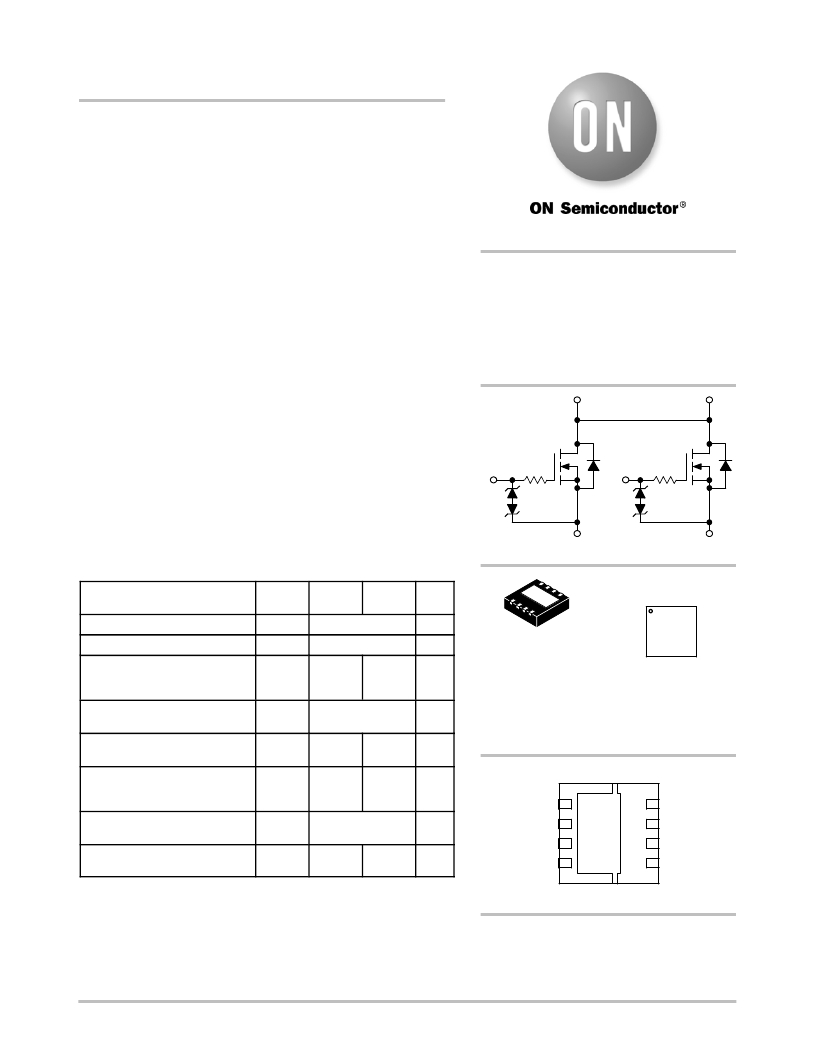
�This� advanced� Power� MOSFET� contains� monolithic� back--to--back�
�Zener� diodes.� These� Zener� diodes� provide� protection� against� ESD� and�
�unexpected� transients.� These� miniature� surface� mount� MOSFETs�
�feature� ultra� low� R� DS(on)� and� true� logic� level� performance.� This� device�
�is� designed� for� use� in� low� voltage,� high� speed� switching� applications�
�where� power� efficiency� is� important.� Typical� applications� are� DC--DC�
�converters,� and� power� management� in� portable� and� battery� powered�
�products� such� as� computers,� printers,� cellular� and� cordless� phones.�
�Features�
�?� Pb--Free� Package� is� Available�
�http://onsemi.com�
�9� AMPERES�
�20� VOLTS�
�R� DS(on)� =� 26� m� Ω�
�(V� GS� =� 4.5� V,� I� D� =� 6.5� A)�
�R� DS(on)� =� 31� m� Ω�
�(V� GS� =� 2.5� V,� I� D� =� 5.8� A)�
�Applications�
�?� Zener� Protected� Gates� Provide� Electrostatic� Discharge� Protection�
�?� Designed� to� Withstand� 4000� V� Human� Body� Model�
�D�
�D�
�?� Ultra� Low� R� DS(on)� Provides� Higher� Efficiency� and� Extends�
�Battery� Life�
�?� Logic� Level� Gate� Drive� --� Can� be� Driven� by� Logic� ICs�
�G� 1�
�2.4� k� Ω�
�G� 2�
�2.4� k� Ω�
�?� Micro8� Leadless� Surface� Mount� Package� --� Saves� Board� Space�
�?� I� DSS� Specified� at� Elevated� Temperature�
�N--Channel�
�S� 1�
�N--Channel�
�S� 2�
�MAXIMUM RATINGS� (T� J� = 25� °� C� unless� otherwise� noted)�
�Steady�
�MARKING� DIAGRAM�
�7900�
�Rating�
�Drain--to--Source� Voltage�
�Gate--to--Source� Voltage�
�Continuous� Drain� Current� (Note� 1)�
�T� A� =� 25� °� C�
�T� A� =� 85� °� C�
�Pulsed� Drain� Current�
�(tp� ≤� 10� m� s)�
�Continuous� Source--Diode�
�Conduction� (Note� 1)�
�Symbol�
�V� DSS�
�V� GS�
�I� D�
�I� DM�
�I� s�
�10� Sec�
�9.0�
�6.4�
�2.9�
�20�
�±� 12�
�30�
�State�
�6.0�
�4.3�
�1.4�
�Unit�
�V�
�V�
�A�
�A�
�A�
�1�
�Micro8� LEADLESS�
�CASE� 846C�
�A�
�Y�
�WW�
�G�
�1�
�AYWW�
�G�
�=� Assembly� Location�
�=� Year�
�=� Work� Week�
�=� Pb--Free� Package�
�Total� Power� Dissipation� (Note� 1)�
�T� A� =� 25� °� C�
�T� A� =� 85� °� C�
�P� D�
�3.2�
�1.7�
�1.5�
�0.79�
�W�
�Drain�
�PIN ASSIGNMEN� T�
�8� 1�
�Source� 1�
�Operating� Junction� and� Storage�
�Temperature� Range�
�Thermal� Resistance� (Note� 1)�
�Junction--to--Ambient�
�T� J� ,� T� stg�
�R� θ� JA�
�--55� to� 150�
�38� 82�
�°� C�
�°� C/W�
�Drain�
�Drain�
�Drain�
�7�
�6�
�5�
�Drain�
�2�
�3�
�4�
�Gate� 1�
�Source� 2�
�Gate� 2�
�Stresses� exceeding� Maximum� Ratings� may� damage� the� device.� Maximum�
�Ratings� are� stress� ratings� only.� Functional� operation� above� the� Recommended�
�Operating� Conditions� is� not� implied.� Extended� exposure� to� stresses� above� the�
�Recommended� Operating� Conditions� may� affect� device� reliability.�
�1.� When� surface� mounted� to� 1� ″� x� 1� ″� FR--4� board.�
�(Bottom� View)�
�ORDERING� INFORMATION�
�See� detailed� ordering� and� shipping� information� in� the� package�
�dimensions� section� on� page� 6� of� this� data� sheet.�
�?� Semiconductor� Components� Industries,� LLC,� 2009�
�October,� 2009� --� Rev.� 7�
�1�
�Publication� Order� Number:�
�NTLTD7900ZR2/D�
�发布紧急采购,3分钟左右您将得到回复。
相关PDF资料
NTLUD3191PZTAG
MOSFET P-CH 20V 1.7A DUAL 6UDFN
NTLUD3A260PZTBG
POWER MOSFET 20V 2A 200 M UDFN6
NTLUF4189NZTAG
MOSFET N-CH 30V 1.2A 6UDFN
NTLUS3192PZTBG
MOSFET P-CH 20V 3.4A SGL 6UDFN
NTLUS3A18PZTBG
MOSFET P-CH 20V 8.2A 6UDFN
NTLUS3A39PZTBG
MOSFET P-CH 20V 5.2A 6UDFN
NTLUS3A40PZTBG
T4 20/8 PCH 2X2 UDFN SING
NTLUS3A90PZTBG
POWER MOSFET 20V 3A 60 MO UDFN6
相关代理商/技术参数
NTLTS3107P
制造商:ONSEMI 制造商全称:ON Semiconductor 功能描述:High Efficiency DC-DC Converters
NTLTS3107P_05
制造商:ONSEMI 制造商全称:ON Semiconductor 功能描述:Power MOSFET -20 V, -8.3 A, Single P-Channel,Micro8 Leadless Package
NTLTS3107PR2G
功能描述:MOSFET PFET 8A PB RoHS:否 制造商:STMicroelectronics 晶体管极性:N-Channel 汲极/源极击穿电压:650 V 闸/源击穿电压:25 V 漏极连续电流:130 A 电阻汲极/源极 RDS(导通):0.014 Ohms 配置:Single 最大工作温度: 安装风格:Through Hole 封装 / 箱体:Max247 封装:Tube
NTLUD3191PZ
制造商:ONSEMI 制造商全称:ON Semiconductor 功能描述:Power MOSFET −20 V, −1.8 A, Cool Dual P−Channel, ESD, 1.6x1.6x0.55 mm UDFN Package
NTLUD3191PZTAG
功能描述:MOSFET PFET WDFN6 20V 1.7A 250mOhm RoHS:否 制造商:STMicroelectronics 晶体管极性:N-Channel 汲极/源极击穿电压:650 V 闸/源击穿电压:25 V 漏极连续电流:130 A 电阻汲极/源极 RDS(导通):0.014 Ohms 配置:Single 最大工作温度: 安装风格:Through Hole 封装 / 箱体:Max247 封装:Tube
NTLUD3191PZTBG
功能描述:MOSFET PFET WDFN6 20V 1.7A 250mOhm RoHS:否 制造商:STMicroelectronics 晶体管极性:N-Channel 汲极/源极击穿电压:650 V 闸/源击穿电压:25 V 漏极连续电流:130 A 电阻汲极/源极 RDS(导通):0.014 Ohms 配置:Single 最大工作温度: 安装风格:Through Hole 封装 / 箱体:Max247 封装:Tube
NTLUD3A260PZ
制造商:ONSEMI 制造商全称:ON Semiconductor 功能描述:Power MOSFET a??20 V, a??2.1 A,Cool Dual Pa??Channel, ESD, 1.6x1.6x0.55 mm UDFN Package
NTLUD3A260PZTAG
功能描述:IGBT 晶体管 POWER MOSFET 20V 2A 200 M RoHS:否 制造商:Fairchild Semiconductor 配置: 集电极—发射极最大电压 VCEO:650 V 集电极—射极饱和电压:2.3 V 栅极/发射极最大电压:20 V 在25 C的连续集电极电流:150 A 栅极—射极漏泄电流:400 nA 功率耗散:187 W 最大工作温度: 封装 / 箱体:TO-247 封装:Tube